2019-09-27
Crystal Orientation and Grain Size: Do They Determine Optoelectronic Properties of MAPbI3 Perovskite?
Publication
Publication
J. Phys. Chem. Lett. , Volume 10 p. 6010- 6018
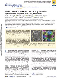
Growing large, oriented grains of perovskite often leads to efficient devices, but it is unclear if properties of the grains are responsible for the efficiency. Domains observed in SEM are commonly misidentified with crystallographic grains, but SEM images do not provide diffraction information. We study methylammoinium lead iodide (MAPbI3) films fabricated via flash infrared annealing (FIRA) and the conventional antisolvent (AS) method by measuring grain size and orientation using electron back-scattered diffraction (EBSD) and studying how these affect optoelectronic properties such as local photoluminescence (PL), charge carrier lifetimes, and mobilities. We observe a local enhancement and shift of the PL emission at different regions of the FIRA clusters, but we observe no effect of crystal orientation on the optoelectronic properties. Additionally, despite substantial differences in grain size between the two systems, we find similar optoelectronic properties. These findings show that optoelectronic quality is not necessarily related to the orientation and size of crystalline domains.
| Additional Metadata | |
|---|---|
| Netherlands Organisation for Scientific Research (NWO) | |
| ACS | |
| doi.org/10.1021/acs.jpclett.9b02757 | |
| J. Phys. Chem. Lett. | |
| Organisation | Hybrid Solar Cells |
|
Muscarella, L., Hutter, E., Sanchez, S., Dieleman, C., Savenije, T., Hagfeldt, A., … Ehrler, B. (2019). Crystal Orientation and Grain Size: Do They Determine Optoelectronic Properties of MAPbI3 Perovskite?. J. Phys. Chem. Lett., 10, 6010–6018. doi:10.1021/acs.jpclett.9b02757 |
|