2021-01-29
Shaping Perovskites: In Situ Crystallization Mechanism of Rapid Thermally Annealed, Prepatterned Perovskite Films
Publication
Publication
ACS Appl. Mater. Interfaces , Volume 13 - Issue 5 p. 6854- 6863
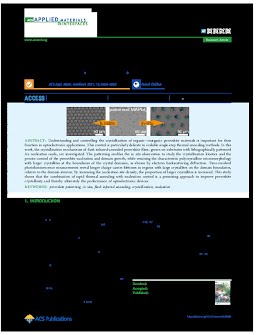
Understanding and controlling the crystallization of organic-inorganic perovskite materials is important for their function in optoelectronic applications. This control is particularly delicate in scalable single-step thermal annealing methods. In this work, the crystallization mechanisms of flash infrared-annealed perovskite films, grown on substrates with lithographically patterned Au nucleation seeds, are investigated. The patterning enables the in situ observation to study the crystallization kinetics and the precise control of the perovskite nucleation and domain growth, while retaining the characteristic polycrystalline micromorphology with larger crystallites at the boundaries of the crystal domains, as shown by electron backscattering diffraction. Time-resolved photoluminescence measurements reveal longer charge carrier lifetimes in regions with large crystallites on the domain boundaries, relative to the domain interior. By increasing the nucleation site density, the proportion of larger crystallites is increased. This study shows that the combination of rapid thermal annealing with nucleation control is a promising approach to improve perovskite crystallinity and thereby ultimately the performance of optoelectronic devices.
| Additional Metadata | |
|---|---|
| ACS | |
| Netherlands Organisation for Scientific Research (NWO) , European Union Research and Innovation Horizon 2020 | |
| doi.org/10.1021/acsami.0c20958 | |
| ACS Appl. Mater. Interfaces | |
| Organisation | Hybrid Solar Cells |
|
Günzler, A., Bermúdez-Ureña, E., Muscarella, L., Ochoa, M., Ochoa-Martínez, E., Ehrler, B., … Steiner, U. (2021). Shaping Perovskites: In Situ Crystallization Mechanism of Rapid Thermally Annealed, Prepatterned Perovskite Films. ACS Appl. Mater. Interfaces, 13(5), 6854–6863. doi:10.1021/acsami.0c20958 |
|
