2021-06-22
Employing Cathodoluminescence for Nanothermometry and Thermal Transport Measurements in Semiconductor Nanowires
Publication
Publication
ACS Nano , Volume 15 - Issue 7 p. 11385- 11395
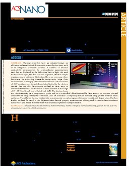
Thermal properties have an outsized impact on efficiency and sensitivity of devices with nanoscale structures, such as in integrated electronic circuits. A number of thermal conductivity measurements for semiconductor nanostructures exist, but are hindered by the diffraction limit of light, the need for transducer layers, the slow scan rate of probes, ultrathin sample requirements, or extensive fabrication. Here, we overcome these limitations by extracting nanoscale temperature maps from measurements of bandgap cathodoluminescence in GaN nanowires of <300 nm diameter with spatial resolution limited by the electron cascade. We use this thermometry method in three ways to determine the thermal conductivities of the nanowires in the range of 19-68 W/m.K, well below that of bulk GaN. The electron beam acts simultaneously as a temperature probe and as a controlled delta-function-like heat source to measure thermal conductivities using steady-state methods, and we introduce a frequency-domain method using pulsed electron beam excitation. The different thermal conductivity measurements we explore agree within error in uniformly doped wires. We show feasible methods for rapid, in situ, high-resolution thermal property measurements of integrated circuits and semiconductor nanodevices and enable electron-beam-based nanoscale phonon transport studies.
| Additional Metadata | |
|---|---|
| , , | |
| ACS | |
| Netherlands Organisation for Scientific Research (NWO) , European Research Council (ERC) | |
| doi.org/10.1021/acsnano.1c00850 | |
| ACS Nano | |
| Organisation | Photonic Materials |
|
Mauser, K., Solà-Garcia, M., Liebtrau, M., Damilano, B., Coulon, P.-M., Vézian, S., Shields, P., Meuret, S.& Polman, A. (2021). Employing Cathodoluminescence for Nanothermometry and Thermal Transport Measurements in Semiconductor Nanowires. ACS Nano, 15(7), 11385–11395.https://doi.org/10.1021/acsnano.1c00850 |
|