2022-01-18
Direct Patterning of CsPbBr3 Nanocrystals via Electron-Beam Lithography
Publication
Publication
ACS Appl. Energy Mater. , Volume 5 - Issue 2 p. 1672- 1680
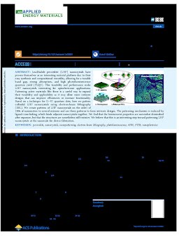
Lead-halide perovskite (LHP) nanocrystals have proven themselves as an interesting material platform due to their easy synthesis and compositional versatility, allowing for a tunable band gap, strong absorption, and high photoluminescence quantum yield (PLQY). This tunability and performance make LHP nanocrystals interesting for optoelectronic applications. Patterning active materials like these is a useful way to expand their tunability and applicability as it may allow more intricate designs that can improve efficiencies or increase functionality. Based on a technique for II–VI quantum dots, here we pattern colloidal LHP nanocrystals using electron-beam lithography (EBL). We create patterns of LHP nanocrystals on the order of 100s of nanometers to several microns and use these patterns to form intricate designs. The patterning mechanism is induced by ligand cross-linking, which binds adjacent nanocrystals together. We find that the luminescent properties are somewhat diminished after exposure, but that the structures are nonetheless still emissive. We believe that this is an interesting step toward patterning LHP nanocrystals at the nanoscale for device fabrication.
| Additional Metadata | |
|---|---|
| , , , , | |
| ACS | |
| Netherlands Organisation for Scientific Research (NWO) , FP7/2007–2013 | |
| doi.org/10.1021/acsaem.1c03091 | |
| ACS Appl. Energy Mater. | |
| Organisation | Hybrid Solar Cells |
|
Dieleman, C., van der Burgt, J., Thakur, N., Garnett, E.& Ehrler, B. (2022). Direct Patterning of CsPbBr3 Nanocrystals via Electron-Beam Lithography. ACS Appl. Energy Mater., 5(2), 1672–1680.https://doi.org/10.1021/acsaem.1c03091 |
|