2022-08-09
Nanopatterning of Perovskite Thin Films for Enhanced and Directional Light Emission
Publication
Publication
ACS Appl. Mater. Interfaces , Volume 14 - Issue 33 p. 38067- 38076
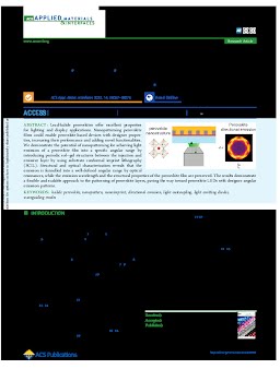
Lead-halide perovskites offer excellent properties for lighting and display applications. Nanopatterning perovskite films could enable perovskite-based devices with designer properties, increasing their performance and adding novel functionalities. We demonstrate the potential of nanopatterning for achieving light emission of a perovskite film into a specific angular range by introducing periodic sol–gel structures between the injection and emissive layer by using substrate conformal imprint lithography (SCIL). Structural and optical characterization reveals that the emission is funnelled into a well-defined angular range by optical resonances, while the emission wavelength and the structural properties of the perovskite film are preserved. The results demonstrate a flexible and scalable approach to the patterning of perovskite layers, paving the way toward perovskite LEDs with designer angular emission patterns.
| Additional Metadata | |
|---|---|
| ACS | |
| Netherlands Organisation for Scientific Research (NWO) , NWO VIDI , EPSRC , NanoLED | |
| doi.org/10.1021/acsami.2c09643 | |
| ACS Appl. Mater. Interfaces | |
| Organisation | Hybrid Solar Cells |
|
Muscarella, L., Cordaro, A., Krause, G.-M., Pal, D., Grimaldi, G., Antony, D., Langhorst, D., Callies, A., Bläsi, B., Höhn, O., Koenderink, F., Polman, A.& Ehrler, B. (2022). Nanopatterning of Perovskite Thin Films for Enhanced and Directional Light Emission. ACS Appl. Mater. Interfaces, 14(33), 38067–38076.https://doi.org/10.1021/acsami.2c09643 |
|