2017-08-21
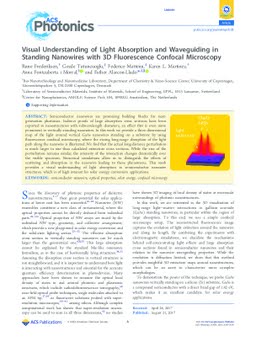
Visual Understanding of Light Absorption and Waveguiding in Standing Nanowires with 3D Fluorescence Confocal Microscopy
Publication
Publication
ACS Photonics , Volume 4 - Issue 9 p. 2235- 2241
Semiconductor nanowires are promising building blocks for nextgeneration photonics. Indirect proofs of large absorption cross sections have been reported in nanostructures with subwavelength diameters, an effect that is even more prominent in vertically standing nanowires. In this work we provide a three-dimensional map of the light around vertical GaAs nanowires standing on a substrate by using fluorescence confocal microscopy, where the strong long-range disruption of the light path along the nanowire is illustrated. We find that the actual long-distance perturbation is much larger in size than calculated extinction cross sections. While the size of the perturbation remains similar, the intensity of the interaction changes dramatically over the visible spectrum. Numerical simulations allow us to distinguish the effects of scattering and absorption in the nanowire leading to these phenomena. This work provides a visual understanding of light absorption in semiconductor nanowire structures, which is of high interest for solar energy conversion applications.
| Additional Metadata | |
|---|---|
| ACS | |
| M.W. Knight | |
| doi.org/10.1021/acsphotonics.7b00434 | |
| ACS Photonics | |
| LMPV | |
| Organisation | 3D Photovoltaics |
|
Frederiksen, R., Tütüncüoglu, G., Matteini, F., Martinez, K., Fontcuberta i Morral, A., & Alarcón-Lladó, E. (2017). Visual Understanding of Light Absorption and Waveguiding in Standing Nanowires with 3D Fluorescence Confocal Microscopy. ACS Photonics, 4(9), 2235–2241. doi:10.1021/acsphotonics.7b00434 |
|