2024-11-08
Scalable Microscale Artificial Synapses of Lead Halide Perovskite with Femtojoule Energy Consumption
Publication
Publication
ACS Energy Lett. , Volume 9 p. 5787- 5794
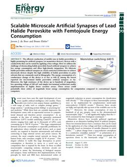
The efficient conduction of mobile ions in halide perovskites is highly promising for artificial synapses (or memristive devices), devices with a conductivity that can be varied by applying a bias voltage. Here we address the challenge of downscaling halide perovskite-based artificial synapses to achieve low energy consumption and allow high-density integration. We fabricate halide perovskite artificial synapses in a back-contacted architecture to achieve microscale devices despite the high solubility of halide perovskites in polar solvents that are commonly used in lithography. The energy consumption of a conductance change of the device is as low as 640 fJ, among the lowest reported for two-terminal halide perovskite artificial synapses so far. Moreover, the high resistance of the device up to hundreds of megaohms, low operating voltage of 100 mV and simple two-terminal architecture enable implementation in highly dense crossbar arrays. These arrays could potentially show orders of magnitude lower energy consumption for computation compared to conventional digital computers.
| Additional Metadata | |
|---|---|
| ACS | |
| European Research Council (ERC) , Netherlands Organisation for Scientific Research (NWO) , European Union Research and Innovation Horizon 2020 | |
| doi.org/10.1021/acsenergylett.4c02360 | |
| ACS Energy Lett. | |
| Organisation | Hybrid Solar Cells |
|
de Boer, J., & Ehrler, B. (2024). Scalable Microscale Artificial Synapses of Lead Halide Perovskite with Femtojoule Energy Consumption. ACS Energy Lett., 9, 5787–5794. doi:10.1021/acsenergylett.4c02360 |
|
